Leave Your Message

What Is a Pitch Btb Connector and How Does It Work?

A Pitch Btb Connector is a compact board-to-board interconnect used to join two printed circuit boards. Its “pitch” describes the center-to-center distance between adjacent contacts. Common pitches include 0.4 mm, 0.5 mm, and 0.8 mm. A smaller pitch saves space, but it also demands tighter manufacturing control.

Dr. Eric Bogatin, a respected signal-integrity engineer, explains, “A connector is part of the transmission line, not an interruption in it.” This principle matters when high-speed signals pass through a Pitch Btb Connector. Each contact, housing cavity, and mating interface can influence impedance, crosstalk, insertion loss, and return loss. A practical design review should examine the connector’s current rating, voltage rating, mating cycles, contact plating, and operating temperature. Datasheets help, but they do not replace testing.

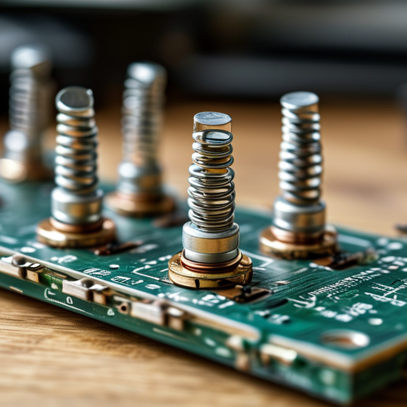
Inside the connector, spring contacts press against matching pads or terminals. This pressure creates the electrical path between the boards. Some designs use stacking heights to control the gap between boards. Others include guide posts or alignment features to prevent uneven mating. Small misalignment can damage fine contacts. It happens more easily than many teams expect.

A reliable selection also considers vibration, dust, assembly tools, and rework conditions. Engineers should inspect sample connectors under magnification. They should measure continuity after repeated mating cycles. The uncomfortable truth is that a connector may pass a basic test and still fail in a real product. This guide examines how a Pitch Btb Connector works, where its limitations appear, and which specifications deserve careful attention before production.

What Is a Pitch Btb Connector and How Does It Work?

What Is a Pitch BTB Connector?

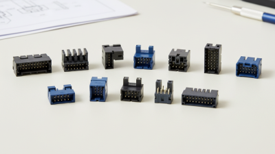
A pitch BTB connector is a board-to-board connector defined partly by its pitch, or the distance between neighboring contact centers. BTB means board-to-board. It joins two printed circuit boards without using a cable. Common pitches include 0.4 mm, 0.5 mm, and 0.8 mm, although other sizes are available.

The connector normally has a plug and a receptacle. One side carries projecting contacts, while the other side receives them. When the boards move together, the contacts create a controlled electrical path between circuits.

The housing maintains alignment and protects the terminals. It may also set a fixed board spacing, called the stack height. Small alignment guides help, but they cannot correct severe installation errors.

Pitch affects more than physical size. A finer pitch saves space but demands tighter manufacturing control and cleaner assembly. It can also make inspection and repair more difficult. Designers must check current capacity, mating cycles, contact resistance, and signal performance. High-speed signals may require carefully managed grounding and impedance. In real assemblies, slight board warpage can cause uneven contact pressure. That detail is easy to overlook. The term “pitch BTB connector” is also not perfectly standardized, so engineers should confirm the drawing, pitch, mating height, and contact arrangement before selection.

How Pitch and Contact Spacing Define Connector Design

What Is a Pitch BTB Connector and How Does It Work?

A pitch BTB connector joins two printed circuit boards without using cables. BTB means board-to-board. The connector uses mating contacts, guides, and housings to maintain an accurate electrical path. Pitch is the center-to-center distance between neighboring contacts. Common designs use fine spacing to save board area, while wider spacing allows easier assembly and stronger mechanical tolerance.

Contact spacing directly shapes the connector design. A 0.4 mm pitch can support compact devices, but it leaves little room for contact walls and inspection tools. Smaller gaps may increase crosstalk, soldering risk, and alignment sensitivity. Designers must also consider contact length, insertion force, current capacity, and mating cycles. A tighter pitch is not automatically better. In practical connector reviews, a small dimensional error can create uneven contact pressure or an intermittent signal. That detail is easy to underestimate.

Tips: Check pitch with a drawing or calibrated microscope. Do not measure from outside edges. Confirm the number of contacts, row spacing, and board thickness together. Leave enough housing clearance for assembly variation. High-speed layouts may need grounded contacts between signal lines. Prototype testing is valuable, even when the CAD model looks correct. Some designs still fail after vibration or repeated mating. That is a useful reminder: electrical performance and mechanical reliability must be evaluated as one system.

What Components Make Up a Pitch BTB Connector?

A pitch BTB connector joins two circuit boards without wires or cables. “Pitch” means the center-to-center spacing between neighboring contacts. Common designs use very small spacing, so alignment becomes critical. A small gap matters.

The contact terminals carry electrical signals between the boards. They are usually formed from spring-like conductive metal, allowing controlled wiping action during mating. Each terminal needs enough contact force for stable conductivity, but excessive force can damage the mating surface. The insulator, or housing, holds every terminal in position. It also maintains spacing and prevents accidental contact between adjacent circuits. Precision molding is essential because even slight movement can create intermittent faults.

The mating interfaces connect with a defined insertion height and engagement depth. Some connectors include guide posts, alignment keys, or locking features to reduce sideways movement. A protective shield may control electromagnetic interference in sensitive applications. Solder tails or surface-mount terminals attach the connector to the board, while mounting anchors handle mechanical stress. Engineers should check coplanarity, terminal plating, and housing strength during inspection. The easy mistake is focusing only on contact count. Board flex, dust, and uneven assembly can matter more. A connector may pass an electrical test yet fail after repeated mating. That possibility deserves testing.

How Does a Pitch BTB Connector Transmit Signals?

A pitch BTB connector joins two printed circuit boards through closely spaced contacts. “Pitch” means the center-to-center distance between neighboring contacts. Smaller pitch saves space, but it also demands tighter manufacturing control. During mating, spring contacts press against matching pads on the opposite board. This pressure creates a low-resistance electrical path. A signal travels from a copper trace on one board, through its contact, across the mating interface, and into the trace on the second board. The connector does not create the signal. It carries it.

For high-speed signals, the path is more complicated than a simple metal bridge. Contact shape, pin spacing, dielectric material, and ground-pin placement influence impedance and signal loss. Ground contacts provide a return path and help limit crosstalk between nearby signal contacts. Differential pairs should remain balanced through the connector. Even a small length mismatch can reduce signal quality. No connector is perfectly transparent. Real testing may reveal reflections, contact resistance, or intermittent behavior caused by dust, vibration, or incomplete mating.

Tips: Check the connector’s rated frequency and current before selecting it. Keep high-speed traces short and route them consistently into the contacts. Place ground contacts near sensitive signal pairs. Inspect mating surfaces under magnification when faults appear. A design that works on one prototype may still need tolerance testing across temperature, movement, and repeated mating cycles.

What Factors Guide the Selection of a Pitch BTB Connector?

Selecting a pitch BTB connector starts with the board layout, not the catalog. Pitch defines the distance between contacts and controls routing space, connector width, and assembly difficulty. Fine-pitch parts save valuable area, but they demand tighter PCB tolerances and better inspection. Measure twice.

Electrical requirements guide the next decision. Check the continuous current, operating voltage, contact resistance, and signal frequency. Power contacts may need wider terminals, while high-speed signals require controlled impedance and careful grounding. Crosstalk can increase when contacts sit closely together. A connector rated for laboratory conditions may perform poorly inside a vibrating industrial enclosure. Real operating conditions matter more than attractive specifications.

Mechanical factors deserve equal attention. Confirm the required stack height, mating direction, retention force, and number of mating cycles. Leave enough clearance for tools and visual inspection. Consider temperature changes, humidity, shock, and vibration before approving the design. Contact plating and housing materials should suit the environment. In practice, early estimates are often wrong, especially when tolerances from two boards combine. I have seen a connector fit on paper but fail during angled mating. A prototype with real boards can reveal warping, excessive insertion force, or insufficient retention. Production volume also affects the choice, because manual assembly may tolerate a different pitch than automated placement. Reliability improves when electrical, mechanical, and manufacturing requirements are reviewed together.

What Is a Pitch BTB Connector and How Does It Work? — Factors That Guide Selection

Selection Factor Typical Data or Range How It Affects Connector Selection How It Works in a BTB Application
Contact Pitch Common miniature pitches include 0.35 mm, 0.40 mm, 0.50 mm, 0.80 mm, and 1.00 mm. Choose the smallest pitch that satisfies routing, current, voltage, manufacturability, and inspection requirements. Smaller pitch saves board area but reduces tolerance for misalignment and contamination. The pitch is the center-to-center distance between adjacent contacts. It determines connector width, contact density, and the spacing available for electrical insulation.
Board-to-Board Arrangement Parallel, coplanar, or perpendicular board configurations. Select a mating geometry that matches the mechanical relationship between the two printed circuit boards and the required assembly direction. A plug section on one board mates with a receptacle section on another board, creating removable electrical and mechanical continuity between the boards.
Stacking Height Typical miniature systems may offer approximately 3 mm to 20 mm of board-to-board spacing. The required height depends on component clearance, heat dissipation, enclosure dimensions, and cable-free board integration. The connector's insulator and terminal geometry maintain a defined gap between boards while preserving contact engagement.
Number of Positions Available configurations range from a few contacts to several hundred contacts, depending on pitch and connector size. Calculate the total number of power, ground, control, and high-speed signal paths, then include spare positions where serviceability or future expansion is important. Each position contains an individual conductive terminal. The mating halves connect corresponding terminals when the boards are assembled.
Current Rating Miniature signal contacts commonly handle below 1 A per contact, while larger power contacts may support several amperes. Use the manufacturer's derating curves, conductor size, temperature rise limits, and the number of simultaneously energized contacts. Do not select by nominal current alone. Current flows through the mated contact interface. Lower resistance and adequate contact normal force help limit heat generation and voltage drop.
Operating Voltage and Insulation Low-voltage electronic systems commonly operate from a few volts to several tens of volts; the actual rating depends on spacing and insulation design. Verify working voltage, dielectric withstand, creepage, clearance, pollution level, and applicable safety requirements for the end product. The housing separates adjacent terminals and prevents unintended arcing or leakage under the specified electrical conditions.
Signal Speed and Impedance Signal suitability depends on contact geometry, differential-pair control, return-path design, and the complete interconnect structure. For high-speed interfaces, evaluate insertion loss, return loss, crosstalk, propagation delay, and impedance continuity rather than relying only on pitch. The connector forms a short transmission-line segment between boards. Changes in geometry can create impedance discontinuities and signal reflections.
Mating and Misalignment Guided systems may provide limited angular, lateral, or floating movement; the allowable amount is design-specific. Choose guided or floating features when board tolerances, blind mating, or automated assembly could produce positional variation. Guide posts, chamfers, and compliant terminals help align the mating halves and absorb limited assembly error without damaging contacts.
Mating Cycles Durability is commonly specified from dozens to thousands of mating cycles, depending on contact plating and construction. Estimate the product's service, test, repair, and manufacturing cycles. Select a higher durability class when repeated disconnection is expected. Spring contacts maintain pressure against the mating surfaces. Wear, plating loss, debris, and loss of normal force can increase contact resistance over time.
Contact Material and Plating Copper-alloy terminals with nickel underplating and a corrosion-resistant contact finish are widely used. Match the plating system to current level, mating cycles, corrosion exposure, fretting risk, and required contact resistance. The conductive terminal carries current, while the surface finish protects the contact interface and supports stable electrical performance.
Temperature Range Many electronic connector systems are designed for approximately −40°C to +85°C, with extended ranges available for demanding applications. Check ambient temperature, self-heating, thermal cycling, material compatibility, and current derating across the full operating range. Housing materials retain insulation and mechanical strength while terminals maintain contact force as temperature changes.
Vibration and Shock Requirements vary by product category, with automotive, industrial, aerospace, and portable equipment generally requiring different test severities. Consider positive locks, board anchors, robust guides, contact retention, and qualification testing appropriate to the installation environment. Mechanical retention prevents separation, while contact spring force helps maintain electrical continuity during vibration and shock.
Termination and Assembly Method Surface-mount termination is common for compact boards; through-hole or hybrid anchoring may be used when greater mechanical strength is needed. Match the terminal style to PCB thickness, pad design, solder process, inspection capability, placement equipment, and rework strategy. The connector is soldered or otherwise attached to each PCB. The board-side terminals transfer electrical and mechanical loads into the board structure.
Housing Material and Flammability High-temperature insulating thermoplastics are commonly selected, often with a specified flame-retardancy classification. Check temperature resistance, dimensional stability, chemical compatibility, flammability requirements, and compliance documentation. The housing positions the terminals, provides electrical insulation, supports guidance, and helps protect the contact interface.
Environmental Protection Open board-to-board connectors are generally intended for controlled environments unless additional shielding or sealing is provided. For dust, moisture, condensation, salt mist, or chemical exposure, verify the complete assembly's protection level and consider a sealed or shielded design. Environmental barriers, when included, reduce the entry of contaminants that could cause corrosion, leakage current, or intermittent contact.
Board Layout and Keep-Out Area The required PCB area includes the connector footprint, courtyard, mating clearance, routing channels, and assembly tooling access. Confirm pad dimensions, polarity marks, keep-outs, component height restrictions, differential-pair routing, and rework access before finalizing the layout. The PCB footprint positions each terminal and provides the electrical paths that connect the BTB interface to surrounding circuitry.

Note: Values shown are representative engineering ranges for selection guidance. Final ratings and qualification requirements must be verified against the specific connector design, PCB layout, operating environment, and applicable standards.