How to Optimize Your High Frequency Connector Design for Maximum Performance
In today's fast-evolving technological landscape, the demand for High Frequency Connectors has surged, driven by the rapid advancements in telecommunications, data centers, and high-speed networking applications. According to a recent report by market research firm Mordor Intelligence, the global High Frequency Connector market is expected to grow at a CAGR of 7.2% from 2021 to 2026, reflecting the increasing need for reliable and efficient connectors that facilitate seamless data transmission. As the frequency of operations increases, optimizing connector design becomes critical to enhance signal integrity and reduce losses. Through careful consideration of factors such as impedance matching, material selection, and mechanical stability, engineers can achieve maximum performance in their High Frequency Connector designs, ensuring scalability and longevity in high-demand environments. This blog will delve into essential tips and strategies for achieving the best possible outcomes in High Frequency Connector optimization.
Understanding the Importance of Frequency in Connector Design for Optimal Signal Integrity
In high-frequency connector design, understanding the significance of frequency is crucial for maintaining optimal signal integrity. As signal frequencies increase, the physical characteristics of the connector—such as capacitance, inductance, and resistance—can significantly impact performance. Data from the Radio Frequency (RF) and Microwave Components Market report by MarketsandMarkets indicates that improper connector choices can lead to losses exceeding 20% at frequencies above 6 GHz. This emphasizes the need for careful selection and optimization of connector materials and geometries to minimize these losses, ensuring that the signal remains strong and clear.
Moreover, as the demand for faster data rates continues to surge, with a projected Compound Annual Growth Rate (CAGR) of 12.5% in the global RF connectors market, focusing on frequency-specific design elements becomes even more vital. High-frequency applications in telecommunications and data centers require connectors that not only support higher bandwidths but also maintain low return loss and insertion loss. According to a study published by the Institute of Electrical and Electronics Engineers (IEEE), connectors optimized for frequency can reduce signal degradation significantly, resulting in improved overall system performance. Therefore, aligning connector design with these frequency considerations is essential for achieving robust and reliable signal integrity in modern electronic systems.
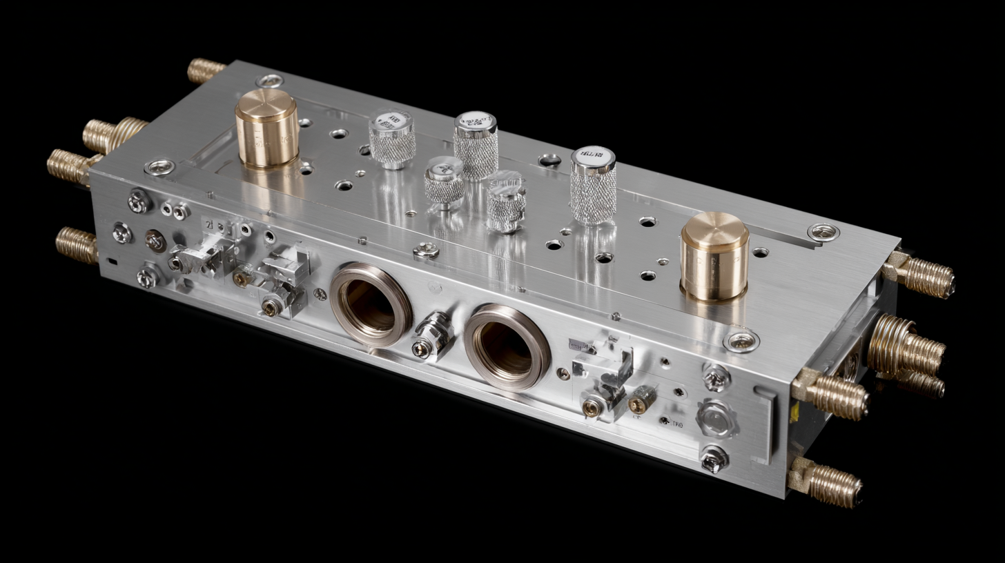
Key Design Parameters that Influence High Frequency Connector Performance
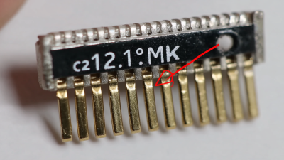
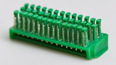
When designing high frequency connectors, several key parameters significantly influence their performance. One of the most crucial factors is the characteristic impedance, which needs to match that of the circuit to minimize reflections and maintain signal integrity. The choice of materials also plays a vital role; selecting low-loss dielectric materials can significantly reduce attenuation, allowing for clearer signal transmission. Additionally, considering the connector geometry, including pin length and spacing, can optimize the electromagnetic performance, as these aspects directly affect impedance and signal propagation.
Another essential design parameter is the return loss, which indicates the efficiency of the connector in reflecting power. A high return loss value is desirable, as it indicates minimal signal loss and better overall performance. Thermal management must also be addressed; ensuring proper heat dissipation can prevent degradation of materials and performance over time. By focusing on these critical design parameters—characteristic impedance, materials selection, geometry, return loss, and thermal considerations—engineers can effectively optimize high frequency connectors for maximum reliability and efficiency in their applications.
How to Optimize Your High Frequency Connector Design for Maximum Performance - Key Design Parameters that Influence High Frequency Connector Performance
| Design Parameter |
Description |
Influence on Performance |
Optimization Technique |
| Impedance Matching |
Ensuring that the impedance of connectors matches the system for minimal signal reflection. |
Reduces insertion loss and enhances overall signal integrity. |
Use precise manufacturing techniques and data simulation during design. |
| Dielectric Material |
The insulating material used between the conductors, affecting signal speed and loss. |
Higher quality dielectrics can significantly lower dielectric loss at high frequencies. |
Select materials with lower dielectric constants and loss tangents. |
| Connector Geometry |
Physical dimensions and layout of the connector pins and housing. |
Affects both the bandwidth and the insertion loss characteristics. |
Employ optimal geometry and minimize length and variation in path. |
| Connector Mating Force |
The force required to connect or disconnect the connector. |
Improper force can lead to contact wear or intermittent connections. |
Optimize spring and latch designs for reliable contact without excessive force. |
| Frequency Range |
The operational range of frequencies for the connector. |
Important for matching the connector to the application’s requirements. |
Identify the target frequency and design connectors to support that range. |
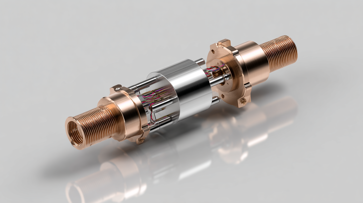
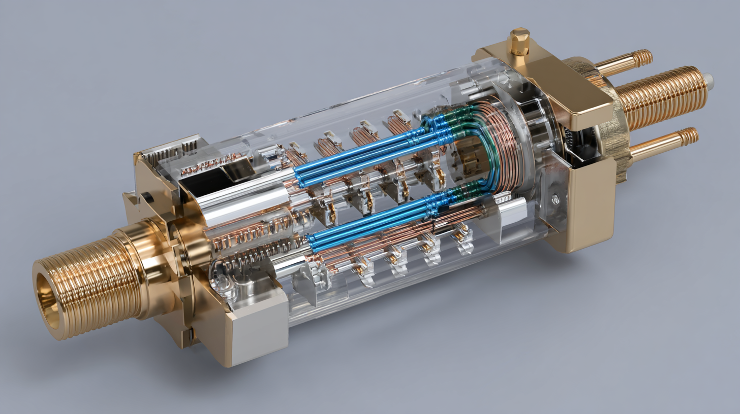
Material Selection Strategies to Enhance High Frequency Connector Functionality
When designing high frequency connectors, the choice of materials is pivotal in enhancing functionality and performance. Materials with excellent electrical conductivity, such as copper or its alloys, are essential to minimize signal loss and ensure efficient transmission. Additionally, selecting materials that can withstand environmental stress, such as corrosion and temperature fluctuations, is critical in maintaining reliability over time, particularly in harsh conditions.
Another important consideration is the dielectric materials used in high frequency connectors. Selecting a dielectric with low loss characteristics can significantly reduce signal attenuation. For instance, materials like PTFE or specific ceramics are often preferred due to their superior insulating properties and ability to maintain performance at high frequencies. The thermal stability of these materials is also crucial, as fluctuations in temperature can affect performance. By carefully considering both the conductive and dielectric elements, designers can create connectors that not only meet high frequency demands but also ensure long-lasting performance and reliability.
Testing and Validation Techniques for High Frequency Connectors in Real-World Applications
When designing high frequency connectors, testing and validation play a crucial role in ensuring optimal performance in real-world applications. It's essential to establish a systematic approach to evaluate the connector's performance under various conditions. This can be achieved through both simulation and practical testing methods. Combining these approaches allows for a comprehensive understanding of how the connector operates in different scenarios, revealing any potential weaknesses that need to be addressed.
Tip: Always utilize vector network analyzers (VNAs) during your testing phase. VNAs help in measuring S-parameters, allowing designers to analyze the frequency response, insertion loss, and return loss of the connectors accurately.
Moreover, thermal and mechanical testing should not be overlooked. High frequency connectors often experience fluctuations in temperature and mechanical stress, which can impact their performance. Conducting durability tests simulates these conditions to ensure that the connectors maintain their integrity and performance standards over time.
Tip: Implement a rigorous environmental testing regimen, including thermal cycling and vibration tests, to ensure your connectors can withstand real-world stresses without failing. This proactive approach will aid in refining your designs for maximum reliability.
Best Practices for PCB Layouts to Complement High Frequency Connector Designs
In optimizing high frequency connector designs, the importance of PCB layouts cannot be overstated. A well-executed PCB layout can significantly enhance signal integrity and overall performance. For example, research indicates that high-speed digital multilayer boards, when designed considering proper grounding and impedance control, can achieve less than 1 dB insertion loss at frequencies upwards of 10 GHz. This performance is critical in applications like automotive wiring harnesses, where signal clarity is essential for reliable power and data transmission.
Moreover, as integration of System-on-Chip (SoC) technologies becomes commonplace, the layout practices must accommodate the unique challenges posed by RF designs. Best practices in RF layout—such as maintaining controlled impedance and minimizing crosstalk—are pivotal. Data suggests that adhering to these strategies can lower electromagnetic interference (EMI) by up to 20 dB, thereby enabling more efficient operation of connected devices. As the demand for high frequency performance in various applications continues to grow, staying informed about these best practices will ensure that designs remain competitive and effective.

 Email
Email WeChat